Some advanced optical technologies cannot be developed further simply because the structure of certain materials prevents them from producing the required optical effects.
In a joint project under the Global Seed Fund programme administered by the MIT Center for International Studies, researchers from Lithuania and the United States will address a fundamental problem: how to overcome crystal symmetry constraints in Weyl semiconductors.
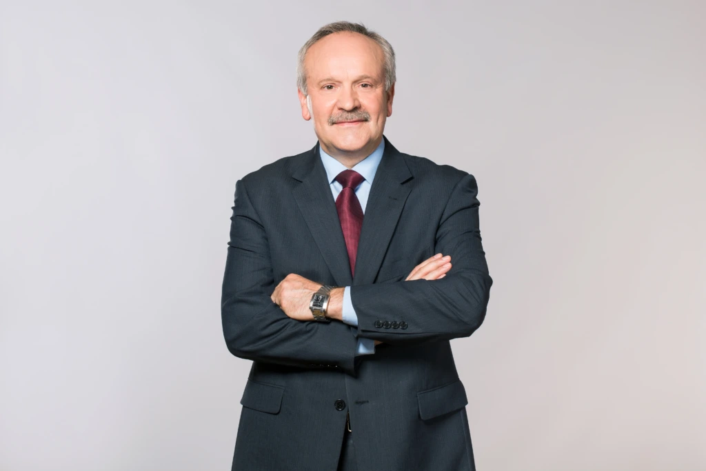
“These constraints prohibit certain nonlinear response mechanisms. Together with our MIT colleagues, we will seek to realise efficient nonlinear optoelectronic responses in practical devices operating at room temperature,” says Prof. Tamulevičius.
The project will explore new ways of giving advanced materials properties they do not normally possess. This could pave the way for more efficient electronics, more precise sensors and new quantum technologies.
Using Light to Break the Symmetry of Structures
Normally, a material responds to light in a predictable way: the more light it receives, the stronger its response. In some systems, however, light can do much more. It can alter the material’s properties and trigger new phenomena.
“Put simply, we are looking at how light and matter interact in unusual, nonlinear ways when the system being studied is not perfectly ordered or symmetrical. Here, ‘symmetry’ means order and uniformity. For example, if something is rotated or flipped, it still looks the same. ‘Symmetry breaking’ means that this order is disrupted, making the system slightly non-uniform or asymmetrical,” explains the KTU professor.
It is precisely in such imperfect, symmetry-broken systems that researchers observe new phenomena with a range of potential applications.
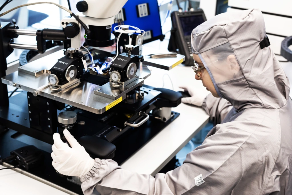
According to Tamulevičius, the team will investigate how light can be used to break the symmetry of a unique crystalline material in nanoscale structures and control both its electrical conductivity and its response to light.
“We will investigate how these effects emerge in nanostructures, namely topological-plasmonic systems, and how symmetry breaking can enable the development of highly sensitive optical detectors,” says the KTU professor.
Possible to Overcome Fundamental Physical Limitations
The researchers will use so-called topological-plasmonic heterostructures. These are structures made from several different materials that combine, within a single system, phenomena characteristic of plasmonics, which studies the collective response of electrons to light, and topological physics, a modern branch of physics that examines not only what a system is made of, but also how its properties depend on its geometric or topological structure.
“These properties make them one of the most promising directions in modern nanophotonics and advanced optoelectronics,” says Tamulevičius.
Unlike existing approaches that rely on impractical experimental conditions, the proposed method uses innovative nanostructures and optically generated vertical electric fields. According to the KTU professor, this could pave the way for integrated, high-efficiency optoelectronic devices.
“Nonlinear optical systems make it possible to realise physical effects that cannot be achieved in linear systems, where the light-induced response is proportional to the intensity of the incoming light. They also help overcome fundamental material symmetry constraints and significantly increase the sensitivity and efficiency of devices,” says the Director of the KTU Institute of Materials Science.
Combining the Strengths of Both Universities
Prof. Tamulevičius will carry out the research together with Dr Svetlana Boriskina, a researcher at the MIT Department of Mechanical Engineering.
“We will combine KTU’s strengths in the self-assembly of plasmonic nanostructures with world-class expertise in topological materials and nonlinear nanophotonics. This synergistic approach gives KTU an opportunity to move from the development of individual nanostructures towards advanced, functional quantum optoelectronic devices,” notes the KTU professor.
The collaboration will also facilitate the exchange of knowledge and expertise, support the development of new research directions, strengthen the competencies of KTU researchers and help train a new generation of highly qualified researchers.
“MIT’s research environment and approach significantly complement the work carried out at KTU, as they provide opportunities to collaborate with leading researchers in fundamental physics, nonlinear optics and topological materials, as well as access advanced experimental infrastructure,” says Tamulevičius.
At the same time, KTU researchers’ expertise in the self-assembly of plasmonic nanostructures and the development of high-performance nanophotonic platforms will help translate these fundamental scientific ideas into practical, engineering-ready solutions.
Laying the Groundwork for Future Technological Breakthroughs
The Director of the KTU Institute of Materials Science notes that fundamental research of this kind can lead to an entirely new generation of technologies offering greater efficiency, sensitivity and functionality than existing solutions.
“It makes it possible to overcome fundamental physical limitations and realise nonlinear optoelectronic effects that have so far been unattainable,” he says.
According to the KTU professor, investment in fundamental research in optics and materials science is essential because it lays the groundwork for future technological breakthroughs.
“Although the practical applications are often not immediately obvious, this type of research enables us to discover new physical phenomena and move beyond existing technological limitations. In this project, that means creating nonlinear optical responses and overcoming material symmetry constraints,” says Tamulevičius.
Historically, many technologies now in widespread use, including semiconductors and lasers, originated in fundamental research. “Investment in this field is therefore critically important for long-term technological competitiveness, innovation and the development of high-value-added solutions,” adds the Director of the KTU Institute of Materials Science.
This project is one of the activities, carried out within the framework of Lithuanian Consortium for cooperation with MIT.